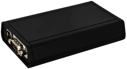
neoECU 20
Device Specifications
neoECU 20 is very similar in function to a neoVI FIRE.
Device Specifications
3 DSPs and 1 RISC processor for 125 MIPS of processing
Power Consumption (typical) : 150mA @ 14.4 VDC
Sleep Power Consumption (typical) : 12mA @ 12.0 VDC
Power Supply: 6-27 Volt Power Operation
Dual user notification LED (red and green)
Temperature Range: -40C to +85C
Vehicle Connectors : 25 Pin male D-SUB and 9 Pin Male D-SUB
Warranty: One Year Limited Warranty
Firmware: Field upgradeable design (flash firmware)
General Purpose IO: 6 MISC IO (0 - 3.3V), 4 IO can be configured as analog
General Purpose IO rate report interval: 10 Hz to 1 kHz or based on digital change
Stand-Alone Mode Including Scripting, Receive Messages, Transmit Messages, Expressions, IO, and Transport Layers
Networks - General
64 Bit time stamping to accuracy of 10 microseconds on CAN and LIN networks and never overflows. 0.5 microsecond accuracy timestamp available if using one network only
Simultaneous operations on all CAN/LIN/J1850 networks
Transmit message double-buffering on all networks allows back to back message transmission
Network Specifications
6x CAN Channels
4 Dedicated ISO11898 Dual Wire CAN Physical Layer (TJA1040)
1 Dedicated ISO11519 Low Speed Fault Tolerant CAN Physical Layer (TJA1054A)
1 Dedicated Single Wire CAN Physical Layer GMW3089 / SAE J2411 (MC33897) CAN 2.0B Active
Up to 1 M-Bit Software Selectable Baud Rate (auto baud capable)
Graphical Bit Time / Baud Rate Calculator
Listen only mode support
High Speed Mode, Test Tool Resistor, and High Voltage Wakeup support
4x LIN (Local Interconnect), ISO9141, Keyword 2000, or K and L Line
Full support for LIN 1.X, 2.X and J2602
LIN J2602 / 2.X compatible physical layer
Software enabled 1K LIN Master Resistor PER CHANNEL
Capable of Generating LIN Waveforms (Including Errors) Using Dedicated Output Compare Hardware (With firmware update)
LIN Bus Monitor Mode identifies errors: Sync Break Error State and Length, Sync Wave Error, Message ID parity, TFrameMax/Slave Not Responding, Checksum Error and Transmit Bit Errors.
LIN Bus Master Mode operates at same time as LIN Bus Monitor
LIN Bus Slave simulation - with or without an LDF file
LIN Bus hardware schedule table with support for LIN diagnostics
UART Based State Machine
only first channel supports L
Programmable Timing Parameters including Inter-Byte, TX Inter-Frame, RX Inter-Frame and Initialization Waveforms (0.5 ms Resolution)
Initialization Waveforms including Fast Init, Five Baud, and Custom
Software Selectable Baud Rate
Software enabled 512K Resistor (channel one only)
1x J1850 VPW (GM Class 2)
VPW Physical Layer capable of TX and RX operations (MC33390)
Reception of IFR data during TX and RX
1x GM CGI
Software Enabled (disables LIN2)
Programmable Bit Rate (625K, 115.2K, others)
Full block mode message reception only
Transmission Option available in CGI Simulation Toolkit

Table 1: neoECU 20 device pinout
1
SW CAN
Single Wire CAN
2
J1850 VPW
J1850 VPW (Class 2)
3
LSFT CAN H
Low Speed Fault Tolerant CAN High
4
LSFT CAN L
Low Speed Fault Tolerant CAN Low
5
MS CAN H
Medium Speed CAN High
6
MS CAN L
Medium Speed CAN Low
7
ISO L
UART/ISO9141/Keyword Line "L"
8
ISO K/LIN 1
UART/ISO9141/Keyword Bi-directional Line "K"
9
DBG CLK
Not Used
10
MISC 1
Miscellaneous Signal 1
11
MISC 2
Miscellaneous Signal 2
12
DBG Data
Not Used
13
PWR GND
Electrical Ground
14
HS CAN H
High Speed CAN High
15
HS CAN L
High Speed CAN Low
16
HS CAN 2 H
High Speed CAN 2 High
17
HS CAN 2 L
High Speed CAN 2 Low
18
MISC 4
Miscellaneous Signal 4
19
HS CAN 3 H
High Speed CAN 3 High
20
HS CAN 3 L
High Speed CAN 3 Low
21
TSYNC CLK H / CGI H
CGI High
22
TSYNC CLK L / CGI L
CGI Low
23
MISC 3
Miscellaneous Signal 3
24
DBG RESET
Not Used
25
VBATT
Electrical Positive Supply 6-27 VDC
Table 2 - neoECU 20, 9 pin Connector Pin Descriptions
1
LIN 1
LIN 1
2
LIN 2
LIN 2
3
LIN 3
LIN 3
4
LIN 4
LIN 4
5
GND
Ground Reference
6
MISC 5
Miscellaneous Signal 5
7
MISC 6
Miscellaneous Signal 6
8
NC
No Connect
9
VBatt Out
No Connect